Case studies
How much does it cost to produce PCBA?
Apr
1. What is PCBA?
PCBA (Printed Circuit Board Assembly) is the process of mounting and soldering electronic components onto a printed circuit board (PCB) to create a functional electronic device. Unlike a bare PCB (which only has copper traces), a PCBA integrates components like resistors, capacitors, ICs, and connectors.
Key Characteristics of PCBA:
✔ Functional electronic unit – Powers devices like smartphones, medical equipment, and IoT gadgets.
✔ Combines PCB fabrication + component assembly – Requires precise soldering (SMT or through-hole).
✔ Must pass quality tests – Ensures reliability (e.g., AOI, ICT, functional testing).
—
2. How is PCBA Manufactured?
The PCBA production process involves 5 critical stages:
Stage 1: PCB Fabrication
– Design: Gerber files define copper layers, holes, and solder masks.
– Production:
– Lamination: Layers of copper and insulation are pressed together.
– Etching: Unwanted copper is removed to form traces.
– Drilling: Holes for vias and component leads are drilled.
Stage 2: Component Sourcing
– Procurement: Components are sourced based on the BOM (Bill of Materials).
– Verification: Authenticity checks to avoid counterfeit parts.
Stage 3: Assembly (SMT & Through-Hole)
– SMT (Surface Mount Technology):
– Components are placed automatically via pick-and-place machines.
– Reflow soldering melts solder paste to attach parts.
– Through-Hole Assembly:
– Components with leads are inserted into holes and wave-soldered.
Stage 4: Testing & Inspection
– AOI (Automated Optical Inspection): Detects soldering defects (bridges, misalignment).
– ICT (In-Circuit Test): Checks electrical connectivity.
– Functional Test: Validates real-world performance.
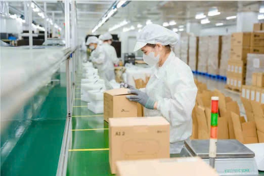
Stage 5: Final Packaging
– Conformal coating (for moisture resistance).
– Boxing and labeling for shipment.
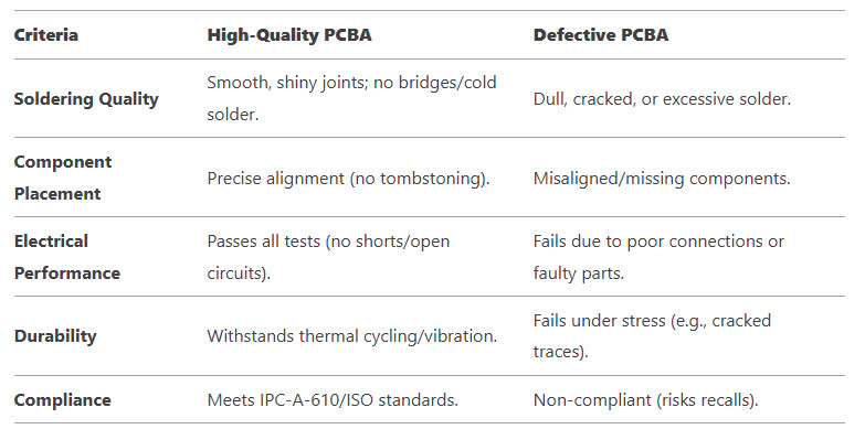
3. Standard-Compliant PCBA vs. Defective PCBA
4. Key Factors Affecting PCBA Manufacturing Costs
Factor 1: PCB Design Complexity
– Layers: 2-layer PCBs are cheapest; 6+ layers cost more.
– Size/Shape: Irregular shapes increase fabrication costs.
– Materials: High-frequency (Rogers) or flexible PCBs are pricier than FR-4.
Factor 2: Component Costs
– Availability: Rare ICs (e.g., automotive-grade MCUs) cost more.
– Packaging: SMD parts are cheaper than through-hole for assembly.
Factor 3: Assembly Process
– SMT: Cost-effective for high volume.
– Mixed (SMT + Through-Hole): Higher labor costs.
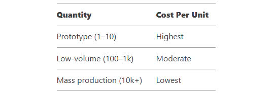
Factor 4: Order Volume
Factor 5: Testing & Certifications
– Basic Testing (AOI): Minimal cost.
– Full Testing (ICT + Functional): Adds 10–20% to price.
– Certifications (ISO 13485, IPC Class 3): Higher compliance = higher cost.
Conclusion: How to Optimize PCBA Costs
1. Simplifying PCB designs – such as reducing layer counts and standardizing components to common SMD sizes – can significantly lower fabrication complexity and material costs while improving manufacturing yield.
2. Ordering PCBA in larger volumes enables manufacturers to offer substantial unit price reductions through economies of scale, while panelizing multiple boards maximizes production efficiency.
3. Selecting experienced PCBA manufacturers with proper certifications and DFM expertise helps prevent costly rework, delays.